Plasmonic Nanostructures: From Resonance to Hot Carriers
Published:
Updated October 10, 2026.
What Is a Plasmon?
What is a plasmon? This was the question I asked the first day I entered graduate school, as I had just switched from a chemistry major. Many papers introduced plasmons as the collective oscillation of electrons as illustrated in Figure 1. Yet I was not entirely satisfied with this definition because two questions were still not answered: 1) why was there a resonance when plasmonic nanostructures were illuminated? 2) why did people always refer to noble metals (e.g., gold, silver) when talking about plasmonic nanostructures? Let’s accept this definition and restrict our attention to noble metals for the time being. An alternative introduction to plasmonic nanostructures and the answers to the two questions can be found using equivalent circuit theory.1
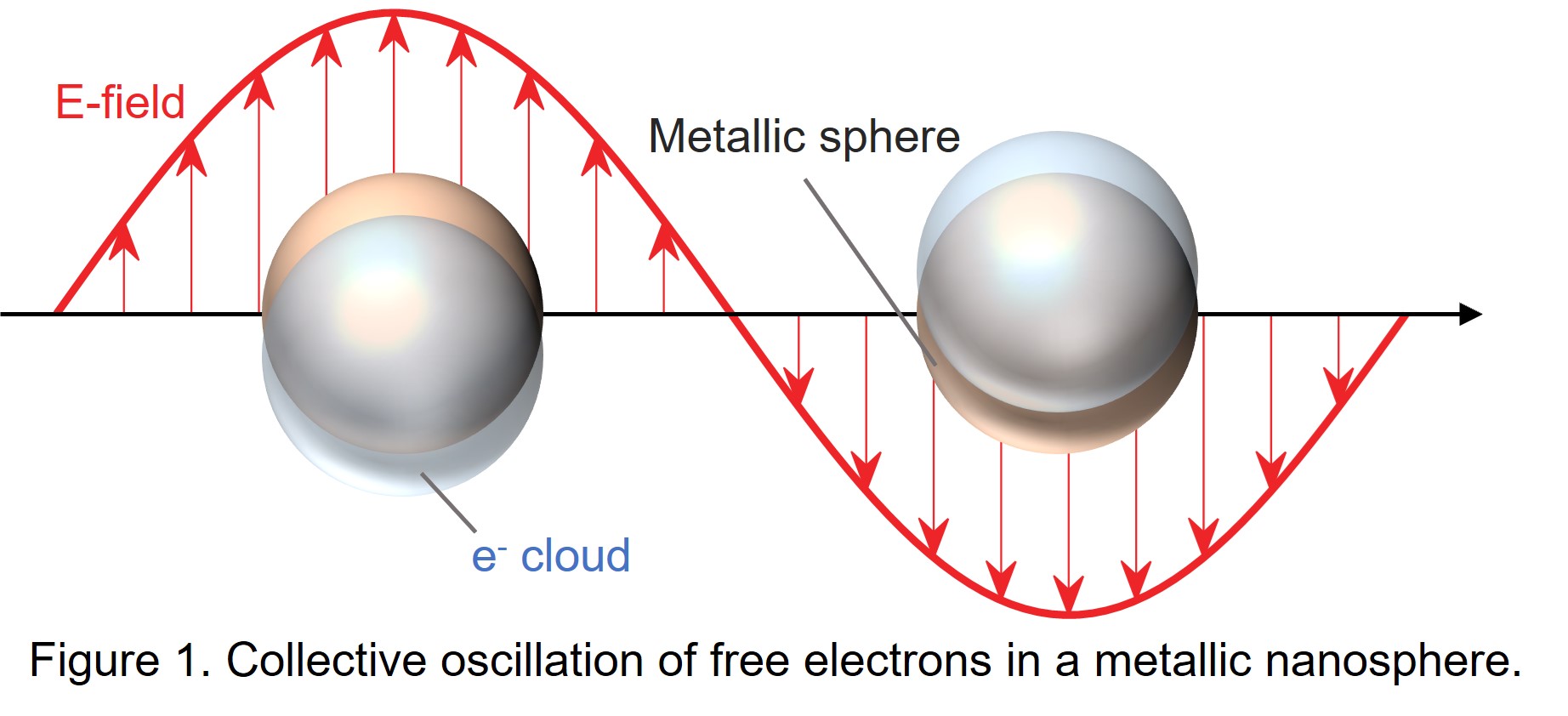
Following this naive rationale, the collective oscillation of free electrons is simply due to the response of electrons (negatively charged particles) to the alternating electric field of light (electromagnetic waves). This oscillation occurs at the metal/dielectric interface and if it is restricted to a nanostructure with a well-defined shape, the localized surface plasmon (LSP) emerges. We call nanostructures that support LSPs plasmonic nanostructures.
Note: There is another type of plasmon (polariton), the surface plasmon polariton (SPP), which can propagate along a surface and is important in nanophotonic applications such as waveguides.
Localized Surface Plasmon Resonance (LSPR)
If one excites a plasmonic nanosphere with broadband illumination, one may find a peak in the absorption or scattering spectrum, which indicates a resonance (LSPR). The wavelength (or frequency) at which this peak occurs is termed the LSPR frequency. Now you can imagine why I was not satisfied with plasmons are the collective oscillations of electrons: oscillations do not necessarily yield a resonance. This dissatisfaction is resolved if we view the plasmonic nanostructure along with its dielectric environment as a nanoscale LC circuit,1 then the LSPR emerges naturally as in an LC resonator. With this in mind, we can imagine that the electrons oscillate much more strongly at the LSPR frequency than off resonance.
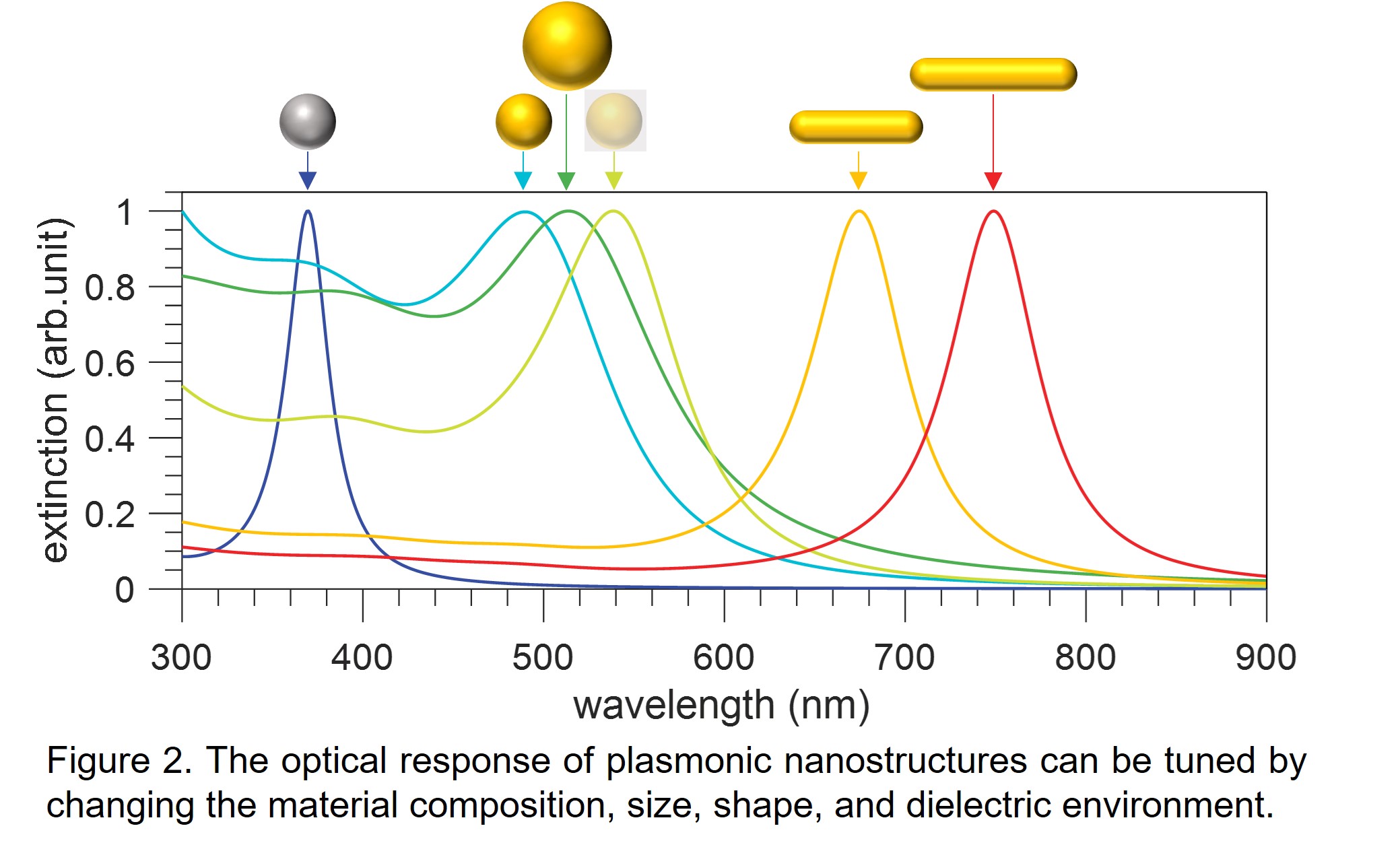
The LSPR can be tailored easily by modifying the composition, size, shape, and dielectric environment (Figure 2). This makes plasmonic nanostructures extremely promising in various applications, such as sensing and photodetection.
Damping of LSPR
What happens after one excites the localized surface plasmon, especially at its LSPR? Of course, we do not expect the oscillation of electrons to last forever as there are many ways for electrons to scatter. It turns out that LSPs can decay through two major damping channels: radiative damping (observed as light scattering) and nonradiative damping (observed as absorption). In addition to these two channels, LSPs can also dephase through scattering with adsorbed molecules or adjacent semiconductors, and this damping channel is identified as chemical interface damping (CID).2
Specifically, I would like to narrow the focus to the nonradiative decay of surface plasmons, which was historically considered a “loss”. While there are continuous efforts to minimize this “loss”, it turns out that the nonradiative decay of surface plasmons may lead to energetic carriers that can be harvested in many fields, e.g., photodetection and photocatalysis.
Dynamics of Plasmonic Nonthermal Carriers
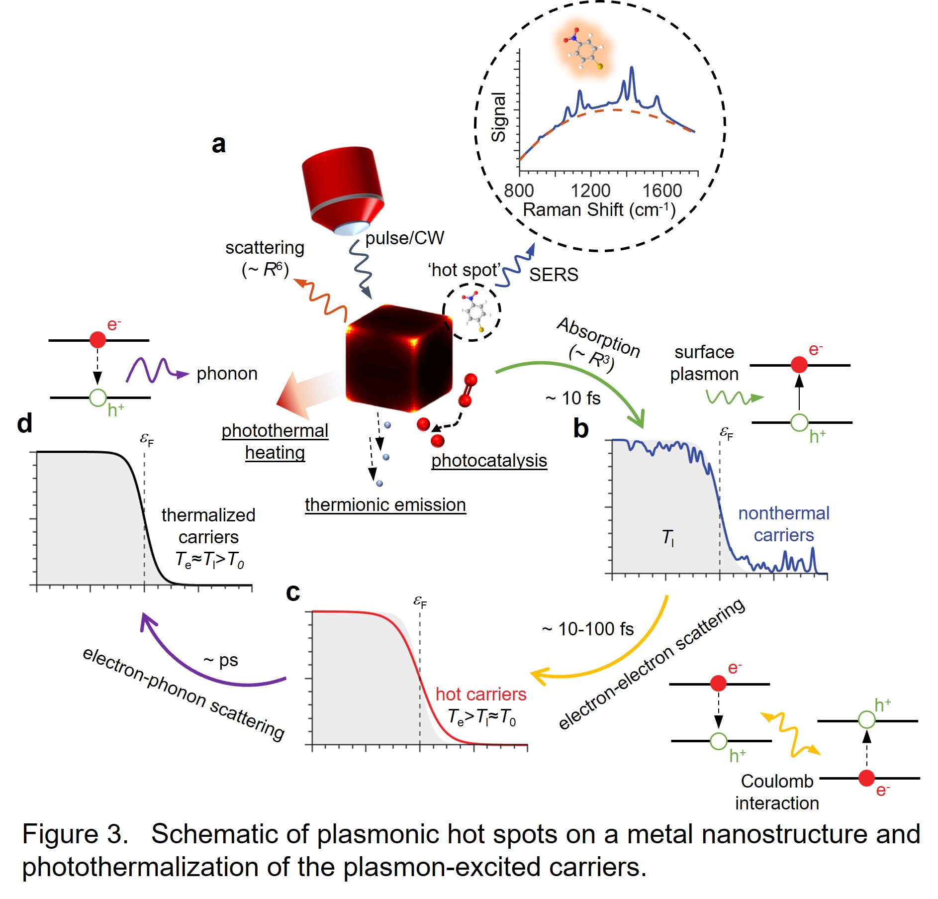
In fact, photothermal heating is just the final stage of the nonradiative decay of surface plasmons (absorption). There are early stages where the plasmonic energy is temporarily stored in the electronic subsystem, rather than in lattice phonons, as shown in Figure 3.3 I prefer to term the carriers (electrons and holes) at the first stage immediately after nonradiative decay the nonthermal carriers (see the tutorial Calculating Plasmon-Induced Hot Carriers from Scratch for calculation examples), as their energy distribution is not a Fermi–Dirac-like distribution. In other words, the energy profile of nonthermal carriers cannot be described using an effective temperature. The nonthermal carriers are extremely short-lived (~100 fs) and relax within the electronic subsystem through electron–electron scattering, and this scattering moves the carriers to the second stage. In the second stage, the carriers still have greater energy compared with lattice phonons, but now their energy profile is Fermi–Dirac-like, so it can be described by an effective temperature $T_e$; these are termed hot carriers. In the final stage (photothermal heating), the electrons are thermalized with phonons through electron–phonon scattering (~ps), and I call these carriers thermalized carriers.
I would like to note here that since both nonthermal carriers and hot carriers are more energetic than thermalized carriers, in much of the literature, people (including me) use hot carriers and nonthermal carriers interchangeably. Part of my research interest lies in utilizing plasmon-induced nonthermal and hot carriers to catalyze (electro)chemical reactions with high yield and selectivity.
References
- Engheta, N., Salandrino, A. & Alù, A. Circuit elements at optical frequencies: nanoinductors, nanocapacitors, and nanoresistors. Phys. Rev. Lett. 95, 095504 (2005).
- Lee, S. A. & Link, S. Chemical interface damping of surface plasmon resonances. Acc. Chem. Res. 54, 1950–1960 (2021).
- Wu, S. & Sheldon, M. Mechanisms of photothermalization in plasmonic nanostructures: insights into the steady state. Annu. Rev. Phys. Chem. 74, 521–545 (2023).